Absolute Maximum Ratings
| Parameter | Rating |
|---|---|
| Input Power Voltage | -0.2 V to 20 V |
| Input Power Current | < 3 A |
| GPIO Pin Voltage | -0.3 V to 2.1 V |
| GPIO Pin Current | -12 mA to 12 mA |
| GPIO Header 1.8V Pin Current | 0 mA to 800 mA |
| RX1 & RX2 Port Input Power (Peak) | < 2.5 dBm |
| RF Ports DC Voltage (If Externally Applied) | -50 V to 50 V |
| GPS Port Active Antenna Current | < 50 mA |
| Operating Temperature Range | -40° C to +85° C |
DC Characteristics
| Parameter | Min | Typ | Max | Units |
|---|---|---|---|---|
| Input Power | 10 | 12 | 15 | V |
| 0.7 | 1 | 1.5 | A | |
| GPIO Input Low, VIL | 0 | 0 | 0.45 | V |
| GPIO Input High, VIH | 1.27 | 1.8 | 1.95 | V |
| GPIO Output Low, VOL | 0 | 0 | 0.45 | V |
| GPIO Output High, VOH | 1.35 | 1.8 | 1.95 | V |
| GPS Port DC Bias | 3.17 | 3.3 | 3.43 | V |
Sampling Characteristics
| Parameter | Min | Typ | Max | Units |
|---|---|---|---|---|
| RX ADC Resolution | 12 | bits | ||
| ADC Sample Rate | 61.44 | Msps | ||
| TX DAC Resolution | 12 | bits | ||
| DAC Sample Rate | 61.44 | Msps | ||
| TX/RX Channel Bandwidth | 0.2 | 56 | MHz |
RF Characteristics
| Parameter | Min | Typ | Max | Units | Notes |
|---|---|---|---|---|---|
| Rx Frequency Range | 70 | 6000 | MHz | ||
| Rx Second-Order Input Intercept Point (IIP2) | 42 | - | 85 | dBm | Varies with gain and Frequency |
| Rx Third-Order Input Intercept Point (IIP3) | -18 | - | 16 | dBm | Varies with gain and Frequency |
| Rx Noise Figure | 2 (800 MHz) | - | 5.2 (6 GHz) | dB | Varies depending on frequency |
| Rx LO Leakage | -128 | - | -92 | dBm | Varies depending on frequency |
| Rx Phase Error | 0.2 | degrees | |||
| Tx Frequency Range | 46.875 | 6000 | MHz | ||
| TX1 & TX2 RF Output Power | -5 | 2 | 9 | dBm | |
| Modulation Accuracy (EVM) | -40 | dB | |||
| Tx Third-Order Input Intercept Point (IIP3) | 0 | - | 28 | dBm | Varies with gain and Frequency |
| Tx Carrier Leakage | -50 | dBc | |||
| Frequency Tolerance | -2 | - | +2 | ppm | |
| Frequency Stability | -1 | - | +1 | ppm |
Physical Characteristics
| Parameter | Typ | Units | Notes |
|---|---|---|---|
| Length | 180 | mm | Including RF connectors |
| 7.09 | in | ||
| 160 | mm | Not including RF connectors | |
| 6.31 | in | ||
| Width | 80 | mm | |
| 3.15 | in | ||
| Height | 26.33 | mm | |
| 1.04 | in | ||
| Weight | 462 | g | |
| 1.02 | lbs | ||
| Kit Shipping Weight | 1.5 | kg | Including case and accessories |
| 3.31 | lbs |
Connector Pinouts
GPIO Port Pinout
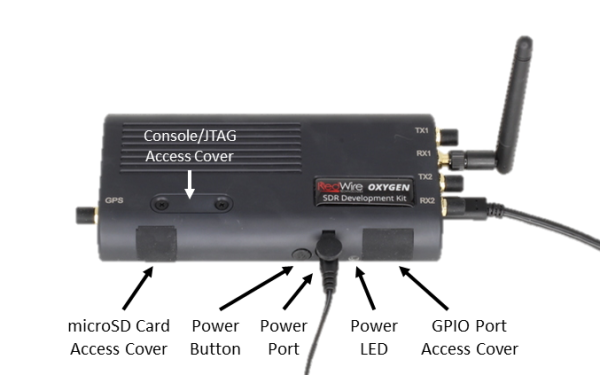
Opening the GPIO port access cover will reveal a 14 pin pluggable header containing 12 GPIO signal lines, 1.8V power, and ground.
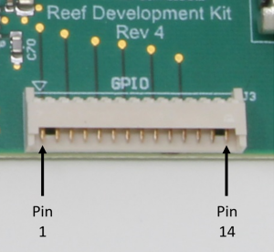
The pinout for the GPIO header is as follows:
| Header Pin Number | Signal Name in Linux OS | FPGA Pin |
|---|---|---|
| 1 | GPIO78 | B64_L1_P |
| 2 | GPIO79 | B64_L7_N |
| 3 | GPIO80 | B64_L3_N |
| 4 | GPIO81 | B64_L8_P |
| 5 | GPIO82 | B64_L3_P |
| 6 | GPIO83 | B64_L8_N |
| 7 | GPIO84 | B65_L15_N |
| 8 | GPIO85 | B64_L9_P |
| 9 | GPIO86 | B65_L15_P |
| 10 | GPIO87 | B64_L9_N |
| 11 | GPIO88 | B65_L7_N |
| 12 | GPIO89 | B64_L4_N |
| 13 | 1.8V | |
| 14 | GND |
The GPIO header uses a 1.25 mm pitch Molex PicoBlade connector (part number 530481410). A cable is provided in the development kit to connect to this header and can be cut in half if flying leads are desired. Molex makes these cables in a variety of standard lengths and the part number for the cable included in the kit is 0151341402.
Console/JTAG Port Pinout
Removing the Console/JTAG access cover reveals a 12 pin header that allows access to the console UART port as well as direct JTAG connection to the FPGA.

The Oxygen SDR allows the FPGA to be reconfigured dynamically during runtime without rebooting using a software routine to program the desired bit file and reload the device tree. As a result, the JTAG port is typically unused but is accessible if needed. The pinout for the header is provided below.
| Header Pin Number | Signal | Direction | Logic Voltage |
|---|---|---|---|
| 1 | GND | - | - |
| 2 | GND | - | - |
| 3 | Console UART Tx | Output | 3.3V |
| 4 | JTAG TCKn | Input | 3.3V |
| 5 | NC | - | - |
| 6 | JTAG VCC Reference | Output | 3.3V |
| 7 | Console UART Rx | Input | 3.3V |
| 8 | JTAG TDOn | Output | 3.3V |
| 9 | NC | - | - |
| 10 | JTAG TDIn | Input | 3.3V |
| 11 | NC | - | - |
| 12 | JTAG TMSn | Input | 3.3V |
The header is recessed into the case and can be difficult to access. For this reason, RWT includes a header extension (ESQ-106-44-L-D) in the kit. For console port and JTAG access, the TE0790 by Trenz Electronics is recommended as it is compatible with Xilinx software tools. If used, the TE0790 should be connected to the extended header in the following orientation.

For simple console port access without JTAG programming, a simple USB to UART adapter can be used. Examples of these include the SparkFun Electronics CH340G Dev 14050, SparkFun Electronics CH340C Dev 15096, and FTDI TTL-232RG-VSW3V3-WE.
The console UART port operates at 115,200 bps, 8 data bits, no parity, 1 stop bit, and no flow control.
Details on how to use these adapters with Oxygen can be found here.
Personality Board Specifications
The Oxygen SDR carrier board has an accessory socket that is intended to accommodate optional RF accessory boards for application specific components such as mixers, filters, amplifiers, etc. Since these modules affect the RF personality of the radio, they are referred to as RF personality boards. The location of the socket on the carrier board and the mezzanine connectors can be seen below.

These boards can be built in either the standard personality board format, or in an extended personality board format if more pcb surface area is needed for components. A schematic template has been created to illustrate the pinout of the mezzanine connectors, how these pin numbers map to the socket connectors, and the power rails that are available.
A full pinout of JRF1 can be seen in the table below. The mezzanine connectors are hermaphroditic and the same part number is used on both the socket and the personality board. This results in even and odd pin numbers being swapped. For example, pin 1 on the socket will connect to pin 2 on the personality board. The JRF2 connector is optional and is currently used only for mechanical support and future expansion of the socket standard. There are no signals on it.
| JRF1 Pin Number (Socket) | Signal Name | Direction | FPGA Pin | Signal Name in Linux OS | Logic Voltage | Mating Connector Pin Number (Personality Board) |
|---|---|---|---|---|---|---|
| 1 | 12VDC | To Personality Board | - | - | - | 2 |
| 2 | 5VDC | To Personality Board | - | - | - | 1 |
| 3 | 12VDC | To Personality Board | - | - | - | 4 |
| 4 | 5VDC | To Personality Board | - | - | - | 3 |
| 5 | GND | - | - | - | - | 6 |
| 6 | GND | - | - | - | - | 5 |
| 7 | 3.3VDC | To Personality Board | - | - | - | 8 |
| 8 | 1.8VDC | To Personality Board | - | - | - | 7 |
| 9 | 3.3VDC | To Personality Board | - | - | - | 10 |
| 10 | 1.8VDC | To Personality Board | - | - | - | 9 |
| 11 | GND | - | - | - | - | 12 |
| 12 | GND | - | - | - | - | 11 |
| 13 | NC | - | - | - | - | 14 |
| 14 | NC | - | - | - | - | 13 |
| 15 | NC | - | - | - | - | 16 |
| 16 | NC | - | - | - | - | 15 |
| 17 | I2C SCL | To Personality Board | MIO28 | I2C Bus 0 | 3.3V | 18 |
| 18 | NC | - | - | - | - | 17 |
| 19 | I2C SDA | Bidirectional | MIO29 | I2C Bus 0 | 3.3V | 20 |
| 20 | NC | - | - | - | - | 19 |
| 21 | GND | - | - | - | - | 22 |
| 22 | GND | - | - | - | - | 21 |
| 23 | NC | - | - | - | - | 24 |
| 24 | NC | - | - | - | - | 23 |
| 25 | NC | - | - | - | - | 26 |
| 26 | NC | - | - | - | - | 25 |
| 27 | GPIO 0 | Bidirectional | B66_L6_N | GPIO94 | 1.8V | 28 |
| 28 | RFIC GPO 0 | To Personality Board | - | - | 3.3V | 27 |
| 29 | GPIO 1 | Bidirectional | B66_L6_P | GPIO95 | 1.8V | 30 |
| 30 | RFIC GPO 1 | To Personality Board | - | - | 3.3V | 29 |
| 31 | GPIO 2 | Bidirectional | B66_L22_P | GPIO96 | 1.8V | 32 |
| 32 | RFIC GPO 2 | To Personality Board | - | - | 3.3V | 31 |
| 33 | GPIO 3 | Bidirectional | B66_L22_N | GPIO97 | 1.8V | 34 |
| 34 | RFIC GPO 3 | To Personality Board | - | - | 3.3V | 33 |
| 35 | GPIO 4 | Bidirectional | B66_L4_P | GPIO98 | 1.8V | 36 |
| 36 | NC | - | - | - | - | 35 |
| 37 | GPIO 5 | Bidirectional | B66_L4_N | GPIO99 | 1.8V | 38 |
| 38 | NC | - | - | - | - | 37 |
| 39 | GND | - | - | - | - | 40 |
| 40 | GND | - | - | - | - | 39 |